DC-DC|Evaluation
Load Regulation
2016.08.25
Points of this article
・A load regulation is indicated as a percentage of change in output voltage with respect to changes in load current, or in terms of a voltage value.
・A load regulation measured on the output pin of a power supply circuit may be different from that which is measured on the power supply pin of a load device.
・Because voltage fluctuations on the power supply pin of a load device may not be desirable, remote sensing should be conducted.
In this section, which is the second section entitled [Evaluating a Switching Regulator], we explain the concept of [Load regulation] and how to measure and evaluate it.
・ Concept of load regulation
Load regulation is a parameter applicable, naturally, to power supply units, as well as to power supply ICs. The term load regulation means the extent to which the output voltage of the power supply changes with respect to changes in load current (output current). As such, it is indicated in terms of a percentage change or in terms of an actual change, such as 10mV. In an ideal world, given that the power supply output voltage is regulated, the voltage should remain constant even when the load current fluctuates. Nevertheless, changes do occur due to the presence of output impedance or line (wire) resistance.
The load regulation varies depending upon whether it is measured on the output pin of a power supply unit or the power supply pin on the load that is connected to the output of power supply unit, that is, an IC to which power is supplied. The load regulation assessed on the output pin of a power supply unit represents the load regulation on the power supply unit itself, and it can be considered as part of the properties of the power supply unit. The load regulation evaluated on the power supply pin of the load device is equal to the power supply characteristic plus a voltage drop due to line resistance from the power supply output pin to the power supply pin of the load device.

As shown in the figure above, the voltage at the power supply pin on the load device simply behaves according to Ohm’s Law. If the line resistance is 0.1Ω, for example, and a 1A load current is taken, the drop in voltage commensurate to the line resistance will be 0.1V. For the 5% accuracy required of a regular 5V/3.3V power supply unit, this will not be a problem. However, in situations where a high degree of accuracy is required, such as 2% in 1V low-voltage power supply units for FPGA and other applications, the performance will not be acceptable. Also, as the current increases, even 5V/3.3V may pose problems. Consequently, when checking the load regulation, it is important to verify whether the voltage on the power supply pin of the load device is within a required accuracy level.
Given this problem, reducing the line resistance may be a conceivable strategy; however, although resistance can be minimized, it cannot be reduced to zero. In other words, in principle decreases in voltage due to line resistance do occur. If the load current increases, an unacceptable condition arises, as would be predicted by calculations. To avoid this problem, a technique of “Remote Sense”may be employed.
By controlling the output voltage by means of feedback loop control, regulated power supply units can maintain a fixed output voltage even in the face of load current fluctuations. In terms of a power supply IC, or in terms of a power supply module, the output is fed back to a pin named FB pin or sense pin, respectively. A critical consideration here is at what point the voltage is to be sensed (fed back). The figure below illustrates the operation of a 1.8V output power supply unit, where the voltage on a power supply output pin is sensed or a load device power supply pin is sensed, in terms of a voltage on the load device power supply pin with respect to the load current, assuming a line resistance of 0.1Ω.

If the voltage on the power supply output pin is sensed (indicated by the red arrow) in a condition in which little line resistance exists, on the power supply output pin a 1.8V level is maintained. However, on load device power supply pins a voltage drop that is equal to load current x line resistance occurs, as would be expected.
When the voltage on the load device power supply pin is sensed (as indicated by the blue arrow), because the voltage on the load device power supply pin is controlled so that it remains at 1.8V, that voltage is maintained irrespective of the load current. In this case, the voltage on the power supply output pin is not equal to 1.8V; rather, it is equal to 1.8V+(load current x line resistance), that is, a voltage level representing the addition of the amount of voltage drop. The sensing of the power supply output voltage on the load pin is referred to as remote sensing. In particular, under high-current, low-voltage conditions, a remote sensing is required.
・Load Regulation and Load Transient Response
The two waveform graphs given below show changes in output voltage when the load current is varied suddenly. Notice that in this evaluation method we look at both the load regulation and the load transient response. The load regulation explained in this section is equal to the voltage corresponding to the constant voltage part of the waveform. This needs to be considered separately, and each part must be addressed differently.
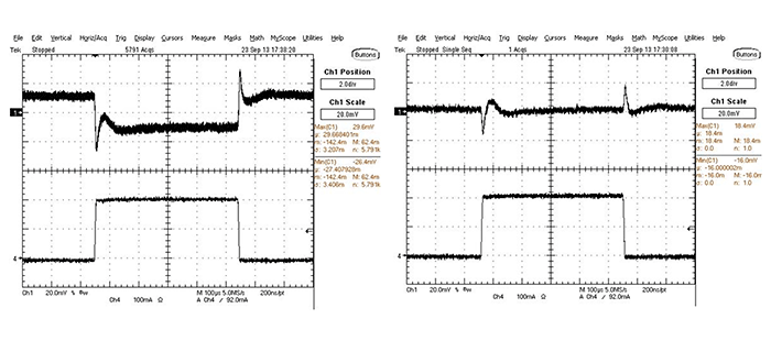
The graph on the left illustrates the case where no remote sensing is performed. The plot at the top represents the output voltage, and the one at the bottom describes the output current. When the load current increases instantaneously from a zero level, because the behavior cannot be accommodated instantaneously, the voltage sags instantaneously. In a short time, the voltage recovers, and a constant voltage resumes, in a behavior which is referred to as a load transient response characteristic. In load regulation, the voltage level that has become constant is evaluated. In this case, the occurrence of a voltage drop is revealed. The graph on the right represents the situation where remote sensing is provided. In this case, there is little change in the constant voltage part.
Load regulation evaluation points may be summarized as follows:
Load Regulation Evaluation Points
- Evaluation items
-Change in output voltage with respect to a change in load current →
Does the changed voltage satisfy required accuracy?
* Also verify any change in ripple voltage with respect to load current fluctuations,
and also check for any abnormal waveforms - Evaluation method
-Measure the output voltage with a voltmeter → Measure the voltage on the load device
power supply pin to determine whether the power supply voltage on the load device is adequate
-Use an oscilloscope to observe the output voltage and waveforms - Condition settings
-Load current: Requires a variable type load device
-emperature: For quick measurements, spot heating/cooling may also be acceptable
【Download Documents】Characteristics and Evaluation Method of Switching Regulators
This handbook reviews the basics of switching regulators and explains how to understand and evaluate the characteristics of switching regulators necessary for design optimization, along with reading and understanding the datasheets of switching regulator ICs.
List of articles related to the「Load Regulation」
Download Technical Documents
Basic of Linear Regulators and Switching Regulators
Basic studies for linear regulators and switching regulators as a DC-DC converter.
DC-DC
- Basic
- Design
-
Evaluation
- Overview of Characteristics and Evaluation Method of Switching Regulators
- How to Read Power Supply IC Datasheets: Cover, Block Diagram, Absolute Maximum Ratings and Recommended Operating Conditions
- Evaluating a Switching Regulator: Output Voltage
-
Introduction
- Definitions and Heat Generation
- Losses in Synchronous Rectifying Step-Down Converters
- Conduction Losses in Synchronous Rectifying Step-Down Converters
- Switching Losses in Synchronous Rectifying Step-Down Converters
- Dead Time Losses in Synchronous Rectifying Step-Down Converters
- Controller IC Power Consumption Losses in a Synchronous Rectifying Step-Down Converter
- Gate Charge Losses in a Synchronous Rectifying Step-Down Converter
- Conduction Losses due to the Inductor DCR
- Example of Power Loss Calculation for a Power Supply IC
- Simplified Method of Loss Calculation
- Heat Calculation for Package Selection: Example 1
- Heat Calculation for Package Selection: Example 2
- Loss Factors
- Matters to Consider When Studying Miniaturization by Raising the Switching Frequency
- Important Matters when Studying High Input Voltage Applications
- Important Matters when Studying Large Output Currents Applications: Part 1
- Important Matters when Studying Large Output Currents Applications: Part 2
- Summary
- Application
- Product Information
- FAQ