AC-DC|Design
Selecting Critical Components: Output Rectifying Diode D4
2018.02.08
Points of this article
・Normally, a device capable of fast switching is used as the output rectifying diode. Here, a fast recovery diode is used.
・An output rectifying diode is in essence selected based on consideration of the rated voltage and losses.
table of contents
This time, we will explain selection of the output rectifying diode.
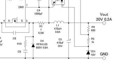
Output Rectifying Diode D4
The output rectifying diode is also called a catch diode or a freewheel diode. In a synchronous rectifying design, this diode is replaced with a transistor, which is called a low-side transistor or the like.
As indicated in the circuit diagram on the right, the output diode D4 is connected from the output to GND. When the high-side MOSFET turns off, energy stored in the inductor is output through D4.
Calculation of Output Diode Component Values
The output rectifying diode turns on and off at the switching frequency, and so a fast recovery diode capable of high-speed switching is used. The rated voltage and losses need to be considered.
The reverse voltage applied to the output diode should be as follows, including a margin.
Vdr = VIN (max)÷0.7 = 372V÷0.7 = 531V → 600V adopted
As a rough estimate, diode losses are as follows.
Pd = VF×Iout = 1V×0.2A = 0.2W
As the diode, a RFN1L6S is used, as specified in the circuit diagram.
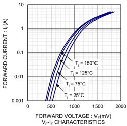
The following are a table of specifications for the fast recovery diode RFN1L6S and the VF-IF characteristic. This time, there is a circuit example, and so there is no need to actually search for a diode; but let us use the opportunity to study this RFN1L6S, on the assumption that we have come across it as a diode with a 600 V rated voltage that can pass 0.2 A or more current.

As the rated voltage, 600 V is the maximum rating for both VR and VRM, agreeing with the calculated value. IO is 0.8 A, and so in terms of performance there is a considerable margin relative to an Iout of 0.2 A, but this much of a margin may be desirable considering the allowable power. Moreover, there may not be component varieties that are an exact match to the design specs. Rather, exact matches are actually rare. In any case, it is necessary to make some compromises, with approximations made in favor of a larger margin.
Calculations were performed with 1 V assumed for VF, but the specs indicate that the maximum values is 1.45 V and the typical value is stipulated to be 1.15 V; the VFーIF characteristic is shown in order to reassure those persons who are wondering whether calculations assuming 1 V for VF are accurate. As a condition for VF, IF is taken to be 0.8 A. In actual use, IF is 0.2 A, and upon determining VF from the graph for an IF of 0.2 A, we see that even under the worst temperature conditions, VF is below 1 V. In other words, these calculations were performed using numerical values close to actual conditions.
How large of a margin to secure will depend on empirical rules. If the margin is too large, the design becomes excessive, so that costs and size may be bloated. Decisions here are not easy, and as in many other areas, will depend on accumulated experience.
We have spoken of empirical rules, but it is essential that losses and junction temperatures be checked under conditions of actual use.
【Download Documents】Methods of Designing Non-isolated PWM Flyback Converter
Explanations how to design a non-isolated buck converter using an AC-DC converter IC, as a next trial.
List of articles related to the「Selecting Critical Components: Output Rectifying Diode D4」
- Overview of Design Examples of AC-DC Non-isolated Buck Converters
- What are Buck Converters? – Basic Operation and Discontinuous Mode vs. Continuous Mode
- Selection of Power Supply ICs and Design Examples
- Selecting Critical Components: Input Capacitor C1 and VCC Capacitor C2
- Selecting Critical Components: Inductor L1
- Selecting Critical Components: Current Sense Resistor R1
- Selecting Critical Components: Output Capacitor C5
- EMI Countermeasures
- Board Layout and Summary
Download Technical Documents
Basic of AC-DC Conversion
Basic studies to understand AC-DC converters and to go designing.
AC-DC
- Basic
-
Design
-
Overview of Design Method of PWM AC-DC Flyback Converters
- Want are Isolated Flyhback Convertors?
- Isolated Flyback Converter Basics: What is Switching AC-DC Conversion?
- Isolated Flyback Converter Basics: What are Characteristics of Flyback Converter?
- Isolated Flyback Converter Basics: Flyback Converter Operation and Snubber
- Isolated Flyback Converter Basics: What are Discontinuous Mode and Continuous Mode?
- Design Procedure
- Determining Power Supply Specifications
- Choosing an IC for Design
- Designing Isolated Flyback Converter Circuits
- Designing Isolated Flyback Converter Circuits: Transformer Design (Calculating numerical values)
- Designing Isolated Flyback Converter Circuits: Transformer Design (Structural Design) – 1
- Designing Isolated Flyback Converter Circuits: Transformer Design (Structural Design) – 2
- Designing Isolated Flyback Converter Circuits: Selecting Critical Components ? MOSFET related – 1
- Designing Isolated Flyback Converter Circuits: Selecting Critical Components ? MOSFET related – 2
- Designing Isolated Flyback Converter Circuits: Selecting Critical Components ? CIN and Snubber
- Designing Isolated Flyback Converter Circuits: Selecting Critical Components ? Output Rectifier and Cout
- Designing Isolated Flyback Converter Circuits: Selecting Critical Components ? VCC of IC
- Designing Isolated Flyback Converter Circuits: Selecting Critical Components – IC Settings Etc.
- Designing Isolated Flyback Converter Circuits: Addressing EMI and Output Noise
- Example Board Layout
- Summary
-
Overview of Design Examples of AC-DC Non-isolated Buck Converters
- What are Buck Converters? – Basic Operation and Discontinuous Mode vs. Continuous Mode
- Selection of Power Supply ICs and Design Examples
- Selecting Critical Components: Input Capacitor C1 and VCC Capacitor C2
- Selecting Critical Components: Inductor L1
- Selecting Critical Components: Current Sense Resistor R1
- Selecting Critical Components: Output Capacitor C5
- Selecting Critical Components: Output Rectifying Diode D4
- EMI Countermeasures
- Board Layout and Summary
-
Introduction
- Design Procedure
- IC Used in Design
- Power Supply Specifications and Replacement Circuit
- Synchronous Rectifying Circuit Section: Selection of Synchronous Rectifying MOSFET
- Synchronous Rectification Circuit Section: Power Supply IC Selection
- Synchronous Rectification Circuit Section: Selection of Peripheral Circuit Components-C1, R3 at MAX_TON Pin, and VCC Pin
- Synchronous Rectification Circuit Section: Selection of Peripheral Circuit Components-D1, R1, R2 at DRAIN Pin
- Shunt Regulator Circuit Section: Selection of Peripheral Circuit Components
- Troubleshooting ①: Case When Secondary-Side MOSFET Suddenly Turns OFF
- Troubleshooting ②: Case When Secondary-Side MOSFET Turns On Due to Resonance Under Light Loading
- Troubleshooting ③: Case When, Due to Surge, VDS2 Rises to Above Secondary-Side MOSFET VDS Voltage
- Comparison of Efficiency of Diode Rectification and Synchronous Rectification
- Points to Note Relating to PCB Layout
- Summary
-
Introduction
- Power Supply ICs Used in Design: Optimized for SiC MOSFETs
- Design Example Circuit
- Transformer T1 Design – 1
- Transformer T1 Design – 2
- Selecting Critical Components: MOSFET Q1
- Selecting Critical Components: Input Capacitor and Balancing Resistor
- Selecting Critical Components: Switch Setting Resistors for Overload Protection Points
- Selecting Critical Components: VCC-Related Components of Power Supply ICs
- Selecting Critical Components: Components Related to Power Supply IC BO (Brownout) Pins
- Selecting Critical Components: Components Related to Snubber Circuits
- Selecting Critical Components: MOSFET Gate Drive Adjustment Circuit
- Selecting Critical Components: Output Rectifying Diode
- Selecting Critical Components: Output Capacitors, Output Setting and Control Components
- Selecting Critical Components: Current Sense Resistors and Components Related to Detection Pins
- Selecting Critical Components: Components for Dealing with EMI and Output Noise
- PCB Layout Example
- Example Circuit and Component List
- Evaluation Results: Efficiency and Switching Waveform
- Summary
-
Overview of Design Method of PWM AC-DC Flyback Converters
- Evaluation
- Product Information
- FAQ