AC-DC|Design
Designing Isolated Flyback Converter Circuits: Selecting Critical Components ? MOSFET related – 1
2016.06.09
Points of this article
・Select a switching transistor (MOSFET) principally based on the drain-source voltage,
the peak current, loss due to on-resistance,and allowable power dissipation for the package.
・Because it is difficult to make a rigorous selection based exclusively on paper and pencil calculations,
you need empirical formulas and measurements on actual devices.
After completing the design of a transformer, we now move on to the switching element. In this section we select a MOSFET Q1 and construct a related circuit.
In the first step, we select a MOSFET Q1 based upon a switching voltage and current. This will be explained in this article [Selecting Critical Components ? MOSFET related – 1].
After that, we determine the circuit (diode D4, resistors R5 and R6) that adjusts the gate drive for the MOSFET. Subsequently, we also determine the current sense resistor R8 that is necessary for current limiting and slope compensation. These items will be explained in the [Selecting Critical Components ? MOSFET related -2] that follows.
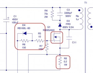
We now describe the operation of the circuit in this part. The signal from the OUT (PWM output) pin of the IC is adjusted in the elements D4, R5, and R6 to ensure that the MOSFET Q1 will operate properly, and that the MOSFET gate is driven. The MOSFET Q1 turns on and off the high voltage that was input to the primary side of the transformer T1 and rectified, and transfers the resulting energy to the secondary side. Turning Q1 on causes the Ids to flow. However, because the current cannot be allowed to flow in unlimited amounts, the resistor R8 is used to sense and limit the current. See the overall circuit described in the section [Designing Isolated Flyback Converter Circuits].
Selecting a MOSFET Q1
The first thing that must be understood is that because selection of MOSFET is difficult to perform based exclusively on a priori calculations, empirical formulas are needed. Ultimately, an actual model is used to verify the extent of derating that is needed, and to determine the MOSFET that must be selected.
For the selection of a MOSFET, the following basic items must be examined:
- Maximum drain?source voltage (Vds)
- Peak current
- Loss due to on-resistance (Ron)
- The maximum allowable power dissipation for the package (Pd)
If empirical formulas are not available, and one cannot make a selection without an adequate basis, we examine both Vds and Ids as follows:
(1) Vds (max)
The value of Vds (max) can be determined from the following equation:
Vds(max) = Vin(max)+VOR+Vspike
=264V×1.41+(12V+1V)×30/6+Vspike=437V+Vspike*
VOR:VO=Vout+VF multiplied by the transformer winding ratio Np:Ns
See「Transformer Design (Calculating numerical values)」
Vin(max): The peak value of the corresponding maximum AC voltage (264V×√2)
Vspike: Spike voltage
*Because Vspike is difficult to calculate, in this example, assuming that a snubber circuit will be added and based on an empirical formula, the value of Vspike is assumed to be 400V or less.
(2) Ids
As general rule, for Ids select a value approximately equal to Ippk×2. From
[Transformer Design (Calculating numerical values)], we obtain Ippk=2.32A.
Or, Ids=2.32×2=4.64A
From this, we select a MOSFET with a value of Vds (max) roughly equal to 800V and an Ids value of 5A. In the example circuit, Rohm’s R8005ANX(800V, 5A) is selected. Also, the on-resistance of this MOSFET is 1.6Ω, and the package is TO-220F.
Subsequently, using this MOSFET in an actual circuit we measure the values for Vds and Ids, and the amount of heat generated to verify whether the level of derating achieved is good enough. Because the lower the input voltage the longer is the MOSFET on-time and the greater is the heat generation due to on-resistance Ron losses, especially in the case of worldwide input (AC85V to AC264V), particular attention is required. A heat sink must be provided as necessary to provide adequate heat dissipation.
Some MOSFET manufacturers provide losses determination methods and a method for estimating such losses. An example is given below for your reference.


By clicking on items beginning with ① indicated as COPY on the home page screen, you can view pages that provide device temperature calculation methods and criteria by which you can assess whether the device is adoption worthy. This information may be useful for checking out a device in an actual device.
This concludes the selection of a MOSFET. The gate drive adjustment circuit and current detection resistors will be explained in [Selecting Critical Components ? MOSFET related -2].
【Download Documents】Design Example for PWM Flyback Converter
ROHM’s seminar materials provided at the seminar venue. Explanation how to design a flyback converter using a power supply IC.
List of articles related to the「Designing Isolated Flyback Converter Circuits: Selecting Critical Components ? MOSFET related – 1」
- Overview of Design Method of PWM AC-DC Flyback Converters
- Want are Isolated Flyhback Convertors?
- Isolated Flyback Converter Basics: What is Switching AC-DC Conversion?
- Isolated Flyback Converter Basics: What are Characteristics of Flyback Converter?
- Isolated Flyback Converter Basics: Flyback Converter Operation and Snubber
- Isolated Flyback Converter Basics: What are Discontinuous Mode and Continuous Mode?
- Design Procedure
- Determining Power Supply Specifications
- Choosing an IC for Design
- Designing Isolated Flyback Converter Circuits
- Designing Isolated Flyback Converter Circuits: Transformer Design (Calculating numerical values)
- Designing Isolated Flyback Converter Circuits: Transformer Design (Structural Design) – 1
- Designing Isolated Flyback Converter Circuits: Transformer Design (Structural Design) – 2
- Designing Isolated Flyback Converter Circuits: Selecting Critical Components ? MOSFET related – 2
- Designing Isolated Flyback Converter Circuits: Selecting Critical Components ? CIN and Snubber
- Designing Isolated Flyback Converter Circuits: Selecting Critical Components ? Output Rectifier and Cout
- Designing Isolated Flyback Converter Circuits: Selecting Critical Components ? VCC of IC
- Designing Isolated Flyback Converter Circuits: Selecting Critical Components – IC Settings Etc.
- Designing Isolated Flyback Converter Circuits: Addressing EMI and Output Noise
- Example Board Layout
- Summary
Download Technical Documents
Basic of AC-DC Conversion
Basic studies to understand AC-DC converters and to go designing.
AC-DC
- Basic
-
Design
-
Overview of Design Method of PWM AC-DC Flyback Converters
- Want are Isolated Flyhback Convertors?
- Isolated Flyback Converter Basics: What is Switching AC-DC Conversion?
- Isolated Flyback Converter Basics: What are Characteristics of Flyback Converter?
- Isolated Flyback Converter Basics: Flyback Converter Operation and Snubber
- Isolated Flyback Converter Basics: What are Discontinuous Mode and Continuous Mode?
- Design Procedure
- Determining Power Supply Specifications
- Choosing an IC for Design
- Designing Isolated Flyback Converter Circuits
- Designing Isolated Flyback Converter Circuits: Transformer Design (Calculating numerical values)
- Designing Isolated Flyback Converter Circuits: Transformer Design (Structural Design) – 1
- Designing Isolated Flyback Converter Circuits: Transformer Design (Structural Design) – 2
- Designing Isolated Flyback Converter Circuits: Selecting Critical Components ? MOSFET related – 1
- Designing Isolated Flyback Converter Circuits: Selecting Critical Components ? MOSFET related – 2
- Designing Isolated Flyback Converter Circuits: Selecting Critical Components ? CIN and Snubber
- Designing Isolated Flyback Converter Circuits: Selecting Critical Components ? Output Rectifier and Cout
- Designing Isolated Flyback Converter Circuits: Selecting Critical Components ? VCC of IC
- Designing Isolated Flyback Converter Circuits: Selecting Critical Components – IC Settings Etc.
- Designing Isolated Flyback Converter Circuits: Addressing EMI and Output Noise
- Example Board Layout
- Summary
-
Overview of Design Examples of AC-DC Non-isolated Buck Converters
- What are Buck Converters? – Basic Operation and Discontinuous Mode vs. Continuous Mode
- Selection of Power Supply ICs and Design Examples
- Selecting Critical Components: Input Capacitor C1 and VCC Capacitor C2
- Selecting Critical Components: Inductor L1
- Selecting Critical Components: Current Sense Resistor R1
- Selecting Critical Components: Output Capacitor C5
- Selecting Critical Components: Output Rectifying Diode D4
- EMI Countermeasures
- Board Layout and Summary
-
Introduction
- Design Procedure
- IC Used in Design
- Power Supply Specifications and Replacement Circuit
- Synchronous Rectifying Circuit Section: Selection of Synchronous Rectifying MOSFET
- Synchronous Rectification Circuit Section: Power Supply IC Selection
- Synchronous Rectification Circuit Section: Selection of Peripheral Circuit Components-C1, R3 at MAX_TON Pin, and VCC Pin
- Synchronous Rectification Circuit Section: Selection of Peripheral Circuit Components-D1, R1, R2 at DRAIN Pin
- Shunt Regulator Circuit Section: Selection of Peripheral Circuit Components
- Troubleshooting ①: Case When Secondary-Side MOSFET Suddenly Turns OFF
- Troubleshooting ②: Case When Secondary-Side MOSFET Turns On Due to Resonance Under Light Loading
- Troubleshooting ③: Case When, Due to Surge, VDS2 Rises to Above Secondary-Side MOSFET VDS Voltage
- Comparison of Efficiency of Diode Rectification and Synchronous Rectification
- Points to Note Relating to PCB Layout
- Summary
-
Introduction
- Power Supply ICs Used in Design: Optimized for SiC MOSFETs
- Design Example Circuit
- Transformer T1 Design – 1
- Transformer T1 Design – 2
- Selecting Critical Components: MOSFET Q1
- Selecting Critical Components: Input Capacitor and Balancing Resistor
- Selecting Critical Components: Switch Setting Resistors for Overload Protection Points
- Selecting Critical Components: VCC-Related Components of Power Supply ICs
- Selecting Critical Components: Components Related to Power Supply IC BO (Brownout) Pins
- Selecting Critical Components: Components Related to Snubber Circuits
- Selecting Critical Components: MOSFET Gate Drive Adjustment Circuit
- Selecting Critical Components: Output Rectifying Diode
- Selecting Critical Components: Output Capacitors, Output Setting and Control Components
- Selecting Critical Components: Current Sense Resistors and Components Related to Detection Pins
- Selecting Critical Components: Components for Dealing with EMI and Output Noise
- PCB Layout Example
- Example Circuit and Component List
- Evaluation Results: Efficiency and Switching Waveform
- Summary
-
Overview of Design Method of PWM AC-DC Flyback Converters
- Evaluation
- Product Information
- FAQ