AC-DC|Design
Designing Isolated Flyback Converter Circuits: Selecting Critical Components ? CIN and Snubber
2016.07.08
Points of this article
・The input capacitor CIN is important to compensate for input currents that are drawn in due to momentary input power shutoffs and switching.
・A snubber circuit is fundamentally essential to protect switching transistors from surges that occur at the input.
table of contents
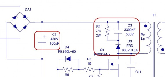
In this section, we discuss the input capacitor C1 and snubber circuit that are positioned at the input. Here the input is a high DC voltage obtained by using a diode bridge to rectify an AC voltage. As indicated in the circuit diagram below, the input capacitor C1 and the snubber circuit R4, C3, D3 are connected to the primary voltage line of the transformer T1, that is, to the diode bridge-rectified voltage.
Upon clicking on the overall circuit diagram in the section [Designing Isolated Flyback Converter Circuits], a separate window opens, to provide information on the overall circuit.
Input capacitor C1
As the input capacitor CIN, a capacitor C1, 450 V/100 μF, is connected. This capacitor has two principal purposes, but it is essentially connected in anticipation of situations in which the input voltage momentarily drops or is cut off.
The first purpose is for when the AC input is momentarily shut off; the input voltage is completely gone, but power can be supplied, albeit for a short period, due to the charge stored on C1. The second purpose has to do with the fact that the MOSFET used as the switching transistor turns large currents on and off extremely rapidly. When the input response cannot keep up with this switching, or when the input impedance is high, the input voltage drops for a short time, and this is augmented by C1. In any case, when the input voltage falls below the required voltage, an anomaly of course occurs in the output voltage, and problems arise in the operation of the circuit to which power is supplied. Although not a perfect solution, the capacitor C1 alleviates such problems.
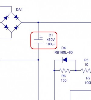
The capacitance of the input capacitor C1 is determined according to the criteria indicated in the table below. Pout is determined from the specifications of this design; calculating based on the table, we have:
C1=2×36W=72μF ⇒ 100μF
| Input voltage (VAC) | CIN(μF) |
|---|---|
| 85-264 | 2×Pout(W) |
| 180-264 | 1×Pout(W) |
The coefficients in this table are for full-wave rectification. The capacitance must be adjusted according to differences in conditions and the specifications for input hold time during momentary shutoffs.
The withstand voltage of the capacitor C1 should be set to the peak value of the input AC voltage. For 264 VAC:
264V×√2=264×1.41=372V ⇒ 400V or higher
Hence the capacitor C1 is selected to be 100 μF and 450 V. As the type of capacitor, electrolytic capacitors are nearly always used.
Snubber circuit: R4, C3, D3
The snubber circuit, configured from a resistor R4, capacitor C3 and diode D3, connects the input line and the MOSFET in the circuit diagram.
In the flyback design, a gap is provided in the transformer core, so that leakage magnetic flux is increased, and a leakage inductance occurs. A switching current flows in this leakage inductance as well, and energy is accumulated, but it is not coupled with the other windings, and so power is not transferred, and a surge voltage occurs across the MOSFET drain and source. When the surge voltage that occurs exceeds the MOSFET voltage rating, there is the possibility of MOSFET failure. In order to prevent this, the snubber circuit is inserted to suppress surge voltages. For details of the snubber circuit, refer to the section [Isolated Flyback Converter Basics: Flyback Converter Operation and Snubber].
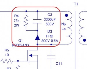
The snubber circuit parameters are determined in the order of (1) the clamping voltage and clamp ripple voltage, (2) R4, (3) C3, and (4) D3.
(1) Determination of clamping voltage (Vclamp) and clamp ripple voltage (Vripple)
The clamping voltage is, as its name implies, a voltage to clamp any surges that occur. It is determined taking into consideration a margin for the MOSFET voltage rating. A MOSFET with 800 V rating was selected. The margin is taken to be 20%. From an empirical rule, the clamp ripple voltage (Vripple) is anticipated to be approximately 50 V.
Vclamp=800V×0.8=640V
Vripple=50V
(2) Determination of R4
R4 is selected based on the following inequality.
![]()
If the leakage inductance Lleak is taken to be 10% of the primary inductance Lp: Lleak
=Lp×10%=249μH×10%=25μH
Substituting values determined in transformer design and the like into the inequality, we have:
![]()
R4 must be smaller than this value, and therefore R4 is set to 75 kΩ.
The value of R4 was determined to be 75 kΩ, and therefore the R4 loss P_R4 is determined. P_R4 can be calculated using the following equation.
![]()
(3) Determination of C3
C3 is determined from the following inequality.
![]()
From the voltage applied to C3, the voltage is set to 640V-264×1.41=268V
⇒ 400 V or higher, including a margin
(4) Determination of D3
Fast operation is required of the diode, and so a fast-recovery diode is used. The withstand voltage is selected to be a voltage equal to or above the MOSFET Vds (max). In the circuit diagram, a diode with a voltage of 800 V is selected.
With this, the resistor R4, capacitor C3, and diode D3 of the snubber circuit are determined. Finally, a surge voltage is affected not only by the transformer leakage inductance, but by the parasitic inductance of printed wiring. Accordingly, with the circuits mounted on a board, the Vds voltage is determined, and the snubber circuit is adjusted as necessary.
The snubber circuit is often fundamentally essential in flyback converters, and its operation and advantages should be understood through repeated evaluations of actual devices and the like.
【Download Documents】Design Example for PWM Flyback Converter
ROHM’s seminar materials provided at the seminar venue. Explanation how to design a flyback converter using a power supply IC.
List of articles related to the「Designing Isolated Flyback Converter Circuits: Selecting Critical Components ? CIN and Snubber」
- Overview of Design Method of PWM AC-DC Flyback Converters
- Want are Isolated Flyhback Convertors?
- Isolated Flyback Converter Basics: What is Switching AC-DC Conversion?
- Isolated Flyback Converter Basics: What are Characteristics of Flyback Converter?
- Isolated Flyback Converter Basics: Flyback Converter Operation and Snubber
- Isolated Flyback Converter Basics: What are Discontinuous Mode and Continuous Mode?
- Design Procedure
- Determining Power Supply Specifications
- Choosing an IC for Design
- Designing Isolated Flyback Converter Circuits
- Designing Isolated Flyback Converter Circuits: Transformer Design (Calculating numerical values)
- Designing Isolated Flyback Converter Circuits: Transformer Design (Structural Design) – 1
- Designing Isolated Flyback Converter Circuits: Transformer Design (Structural Design) – 2
- Designing Isolated Flyback Converter Circuits: Selecting Critical Components ? MOSFET related – 1
- Designing Isolated Flyback Converter Circuits: Selecting Critical Components ? MOSFET related – 2
- Designing Isolated Flyback Converter Circuits: Selecting Critical Components ? Output Rectifier and Cout
- Designing Isolated Flyback Converter Circuits: Selecting Critical Components ? VCC of IC
- Designing Isolated Flyback Converter Circuits: Selecting Critical Components – IC Settings Etc.
- Designing Isolated Flyback Converter Circuits: Addressing EMI and Output Noise
- Example Board Layout
- Summary
Download Technical Documents
Basic of AC-DC Conversion
Basic studies to understand AC-DC converters and to go designing.
AC-DC
- Basic
-
Design
-
Overview of Design Method of PWM AC-DC Flyback Converters
- Want are Isolated Flyhback Convertors?
- Isolated Flyback Converter Basics: What is Switching AC-DC Conversion?
- Isolated Flyback Converter Basics: What are Characteristics of Flyback Converter?
- Isolated Flyback Converter Basics: Flyback Converter Operation and Snubber
- Isolated Flyback Converter Basics: What are Discontinuous Mode and Continuous Mode?
- Design Procedure
- Determining Power Supply Specifications
- Choosing an IC for Design
- Designing Isolated Flyback Converter Circuits
- Designing Isolated Flyback Converter Circuits: Transformer Design (Calculating numerical values)
- Designing Isolated Flyback Converter Circuits: Transformer Design (Structural Design) – 1
- Designing Isolated Flyback Converter Circuits: Transformer Design (Structural Design) – 2
- Designing Isolated Flyback Converter Circuits: Selecting Critical Components ? MOSFET related – 1
- Designing Isolated Flyback Converter Circuits: Selecting Critical Components ? MOSFET related – 2
- Designing Isolated Flyback Converter Circuits: Selecting Critical Components ? CIN and Snubber
- Designing Isolated Flyback Converter Circuits: Selecting Critical Components ? Output Rectifier and Cout
- Designing Isolated Flyback Converter Circuits: Selecting Critical Components ? VCC of IC
- Designing Isolated Flyback Converter Circuits: Selecting Critical Components – IC Settings Etc.
- Designing Isolated Flyback Converter Circuits: Addressing EMI and Output Noise
- Example Board Layout
- Summary
-
Overview of Design Examples of AC-DC Non-isolated Buck Converters
- What are Buck Converters? – Basic Operation and Discontinuous Mode vs. Continuous Mode
- Selection of Power Supply ICs and Design Examples
- Selecting Critical Components: Input Capacitor C1 and VCC Capacitor C2
- Selecting Critical Components: Inductor L1
- Selecting Critical Components: Current Sense Resistor R1
- Selecting Critical Components: Output Capacitor C5
- Selecting Critical Components: Output Rectifying Diode D4
- EMI Countermeasures
- Board Layout and Summary
-
Introduction
- Design Procedure
- IC Used in Design
- Power Supply Specifications and Replacement Circuit
- Synchronous Rectifying Circuit Section: Selection of Synchronous Rectifying MOSFET
- Synchronous Rectification Circuit Section: Power Supply IC Selection
- Synchronous Rectification Circuit Section: Selection of Peripheral Circuit Components-C1, R3 at MAX_TON Pin, and VCC Pin
- Synchronous Rectification Circuit Section: Selection of Peripheral Circuit Components-D1, R1, R2 at DRAIN Pin
- Shunt Regulator Circuit Section: Selection of Peripheral Circuit Components
- Troubleshooting ①: Case When Secondary-Side MOSFET Suddenly Turns OFF
- Troubleshooting ②: Case When Secondary-Side MOSFET Turns On Due to Resonance Under Light Loading
- Troubleshooting ③: Case When, Due to Surge, VDS2 Rises to Above Secondary-Side MOSFET VDS Voltage
- Comparison of Efficiency of Diode Rectification and Synchronous Rectification
- Points to Note Relating to PCB Layout
- Summary
-
Introduction
- Power Supply ICs Used in Design: Optimized for SiC MOSFETs
- Design Example Circuit
- Transformer T1 Design – 1
- Transformer T1 Design – 2
- Selecting Critical Components: MOSFET Q1
- Selecting Critical Components: Input Capacitor and Balancing Resistor
- Selecting Critical Components: Switch Setting Resistors for Overload Protection Points
- Selecting Critical Components: VCC-Related Components of Power Supply ICs
- Selecting Critical Components: Components Related to Power Supply IC BO (Brownout) Pins
- Selecting Critical Components: Components Related to Snubber Circuits
- Selecting Critical Components: MOSFET Gate Drive Adjustment Circuit
- Selecting Critical Components: Output Rectifying Diode
- Selecting Critical Components: Output Capacitors, Output Setting and Control Components
- Selecting Critical Components: Current Sense Resistors and Components Related to Detection Pins
- Selecting Critical Components: Components for Dealing with EMI and Output Noise
- PCB Layout Example
- Example Circuit and Component List
- Evaluation Results: Efficiency and Switching Waveform
- Summary
-
Overview of Design Method of PWM AC-DC Flyback Converters
- Evaluation
- Product Information
- FAQ